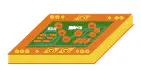
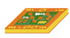
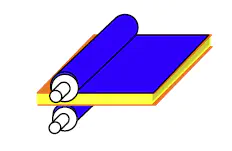
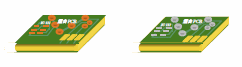
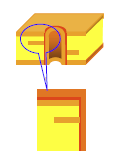
How to make a PCB
When number of layer is greater than two Printed Circuit Boards (PCB) are made by stacking multiples cores and prepreg sheets. Internal layers are manufactured first then outer layers are done at the end.
Process
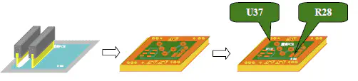
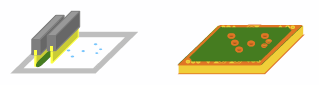
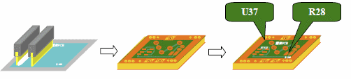
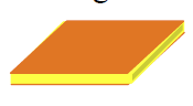
Step 1 : Core
 “Core” sheets are composed by an epoxy resin with a copper sheet on each side. Usually PCB manufacturer receive it already assembled with a photosensitive resin applied on each copper side.
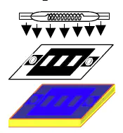
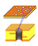
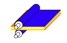
Step 2 : Photomask
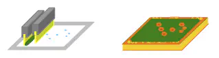
 UV light with photo film are used to print traces and pads on photosensitive resin. Photosensitive resin gets hard when it receives UV light. This process protects copper areas where traces are located.
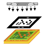
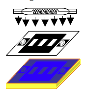
Step 3 : Traces printing
 Non protected copper is dissolved by a chemical bath. Then another bath removes remaining resins.
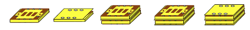
Step 4 : Repeat for each core
 Step one, two and three are repeated to prepare each core. Two times for a six layers PCB, Three times for eight layers PCB, etc..
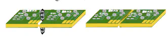
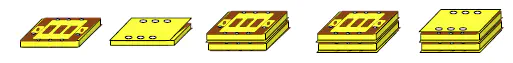
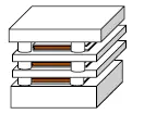
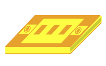
Step 5 : Core stacking
 All cores are stacked with a prepreg isolating sheet between each. The “Prepreg” sheet is made of multiple fiberglass layers glued with resin. The two external layers are created by assembling a copper sheet on top of “prepreg”.
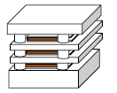
Step 6 : Glue all layers
 All assembled layers are compressed together at high temperature. This allows to harden resin and to glue all layers.
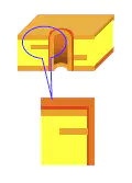
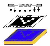
Step 7 : Drill vias
 Vias are drilled using a laser beam or a drilling machine depending on hole size.
Step 8 : Vias plating

 To allow via to conduct between all layers, copper is added inside via holes using electrolysis process. During this step, external layers copper thickness increase also.
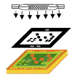
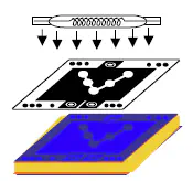
Step 9 : External layers lightmask
 External layers are now printed using UV lighting. This is the same process as for internal layers
Step 10 : Print external layers
 Chemical bath dissolves non protected coper
Step 11 : Apply soldermask
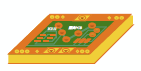
 Soldermask is applied on PCB external layers. This gives PCB final color, it is usually green.
Step 12 : Harden soldermask
 A light mask and a UV light are used to harden solder mask on all PCB except where chips will be welded.
Step 13 : Clean soldermask
 Remaining non hardened soldermask is removed using a chemical bath.
Step 14 : Apply silkscreen
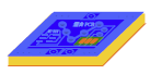
 Silkscreen is applied on external layers
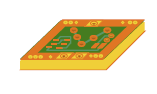
Step 15 : Specific treatments
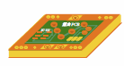
 At this step, it is possible to add some specific treatment like gold plating on part of PCB.
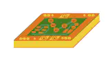
Step 16 : PCB panel cutting


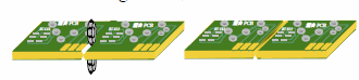
Finally, PCB panel is cut and divided into individual PCB.


